Technical Exploration Series:
VPT’s Technical Exploration series investigates a variety of engineering design concepts that are centered around our core expertise. From deep dives into complex topics, to beginner explanations of concepts for home engineering projects, VPT hopes to provide informative, educational content tailored to specific levels of expertise.
Article Overview:
Topics:
- Introduction to switching in MOSFETs:
- Waveforms during switching
- Calculating Power Loss
- Minimizing Power Loss
Author:
Ray Orr
Complexity:
Advanced
Recommended Pre-requisite knowledge:
- Transistors and Power Electronic Semiconductor Devices
- Electrical Circuit Design and Switching Waveforms
Driving Power MOSFETs: Switching Speed, Switching Frequency and Loss
By: Ray Orr
Switching Waveforms:
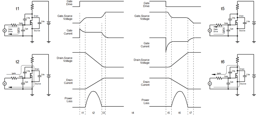
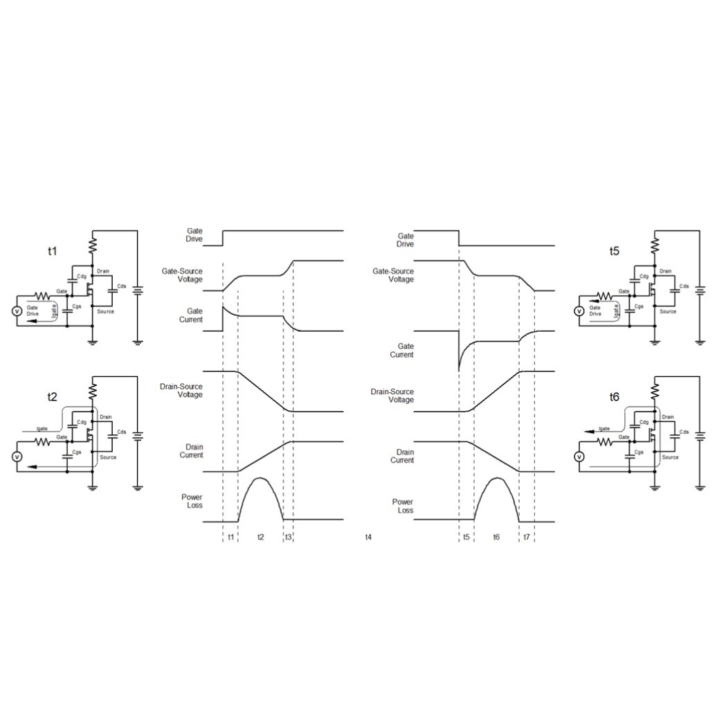
This article is based on the ideas showcased by the waveforms of Figure 1. These illustrate simple but important concepts in the field of power electronics. Namely, the relation between gate drive current, switching speed, frequency and loss in switching MOSFETs.

Figure 1: MOSFET switching waveforms
The four schematic illustrations in the corners of Figure 1 show a MOSFET switching circuit with the drive currents flowing during the time intervals t1, t2, t5 and t6 respectively. The parasitic capacitances of the MOSFET are shown to allow discussion.
The waveforms on the left side are the turn-on waveforms for the MOSFET. The waveforms on the right are the MOSFET turn-off waveforms. The waveforms from the top to the bottom are;
- gate drive signals from the source V
- gate-source voltage
- gate current
- drain-source voltage
- drain current
- instantaneous power during the switching interval
The intervals t1 to t7 are the segments of the waveforms that are discussed in detail.
- At the beginning of t1 the gate drive is driven high from the drive source V. The gate-source voltage rises following the Resistance-Capacitance (RC) curve of the gate resistance and the gate capacitance of the MOSFET. Gate current flows through the input capacitance. The MOSFET remains in the off-state and no drain current flows.
- At the beginning of t2 the gate voltage reaches the gate-source threshold voltage of the MOSFET. At this point drain current begins to flow discharging the drain-source capacitance (Cds) and the drain-gate capacitance (Cdg) aka Miller Capacitance. The negative feedback at the gate from the discharge of Cdg holds the gate at the gate-source threshold. The gate current flows through Cdg. The slew rate of Cdg is determined by the equation I = C dv /dt where I is the gate current. Since the gate voltage is constant during this interval the slew rate of Cds is the same as the slew rate of gate-source capacitance (Cgs). This is seen as a constant rate of change of the drain voltage. The drain current increases linearly as the voltage across the drain resistance increases. The power dissipation is the product of the instantaneous current and voltage. At the end of t2 the drain-source voltage has reached zero.
- At the beginning of t3 the MOSFET is fully on. Cdg is in parallel with Cgs. The gate current begins to flow into both Cds and Cgs causing the gate to rise up to the voltage from the drive source V.
The process is reversed during the interval from the beginning of t5 to the end of t7. During t5 the gate capacitance is discharged down to the gate-source threshold. The gate is held at the gate-source threshold during t6 while the voltage across Cds and the drain-source voltage ramps up. During interval t7 the gate voltage drops to zero.
The on-time of the MOSFET is from the end of t1 to the beginning of t7. The off-time of the MOSFET is from the beginning of t7 to the end of t1.
Calculating Loss:
For illustrative purposes I have assumed some values for the gate curren(IGate), the applied voltage(VDC), the drain resistor (Rdrain), Cdg, Cgs, Cds and the switching frequency (fsw).

These values are used in the calculations shown below. To begin, the rate of change of voltage across the drain-gate capacitor is calculated;

From this slew rate an equation for the drain-source voltage, the drain current and the power dissipated in the MOSFET are developed. In this case, the drain current can be calculated based on the resistor in series with the drain of the MOSFET. In a power converter the drain current will be a function of the circuit topology.

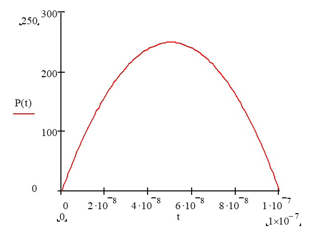
Figure 2 shows the parabolic curve of the instantaneous power dissipation.

Figure 2: Instantaneous power dissipation during the turn-on switching interval
If we integrate the power loss over the switching interval we can calculate the energy lost during the turn-on switching event.

The switching loss of the MOSFET turn-on can be calculated from the turn-on energy and the frequency.

The turn-off losses can be calculated in the same way. The sum of the turn-on loss and the turn-off loss gives us the switching loss. From the calculations we can see that switching loss is directly proportional to frequency and inversely proportional to switching time.
Minimizing Loss:
So why don’t we reduce the switching loss by driving the MOSFET gate with more current or by reducing the frequency? In some cases this is the right choice. However, higher drive current and faster switching edges produce more electromagnetic emissions. With very large MOSFETs, many amperes of drive current may be required. Lowering the switching frequency is also an option. However, all the magnetic components are likely to be larger. This also true of all the filter capacitors. These components largely dictate the size of a power circuit.
Conclusion
Designing efficient power supplies isn’t a walk in the park. Here we just explored a vital part of the puzzle in how to properly drive a switching MOSFET that is turning off and on over 100 000 times per second. While some engineers will spend their entire lives working on researching, optimizing or building MOSFETs, this article has hopefully laid the groundwork needed to begin to understand and maybe even use MOSFETs.


No responses yet